KAUST Solar Platform

About the Platform
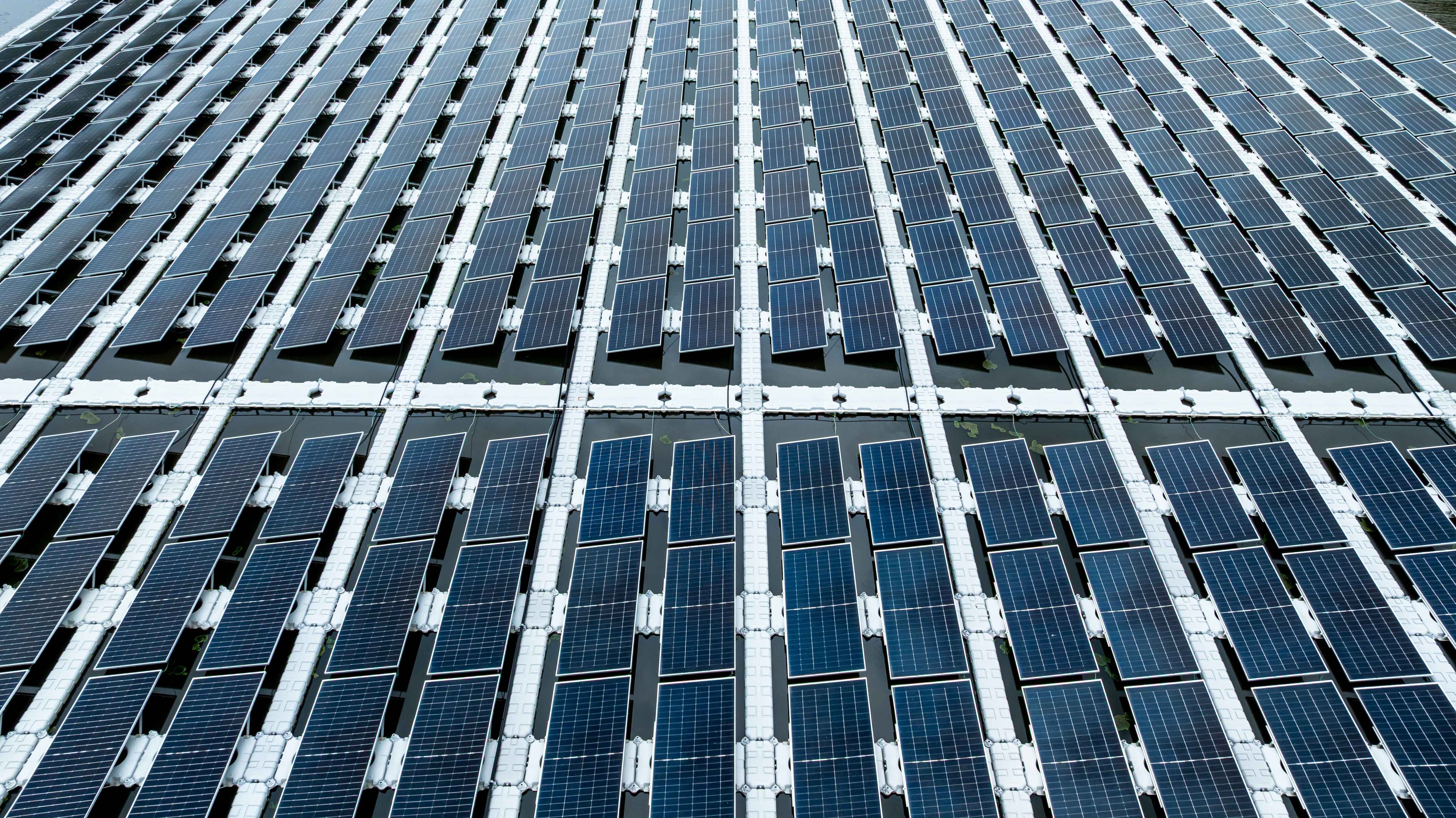
The current expertise in the KAUST Solar Platform is centered on photovoltaic applications based on organic, silicon, and perovskite materials. The Platform capabilities revolve around semiconductor preparation, processing, device fabrication and characterization, with particular emphasis on photovoltaic materials and devices. Some of the research work covers: High-Efficiency Perovskite/Perovskite and Perovskite/Silicon Tandem Solar Cells, Resilient Solution-Processed Photovoltaics, Solar Fuels, Single and Multi-Junction Organic Solar Cells, and more.

Platform Infrastructure
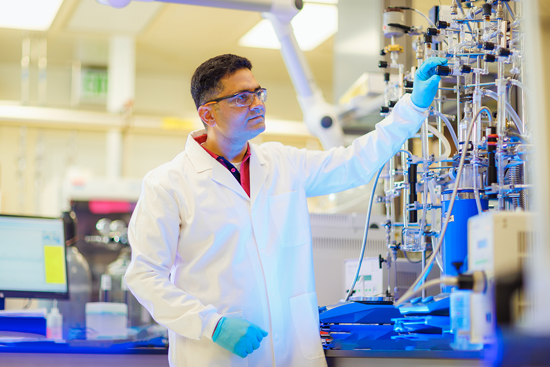
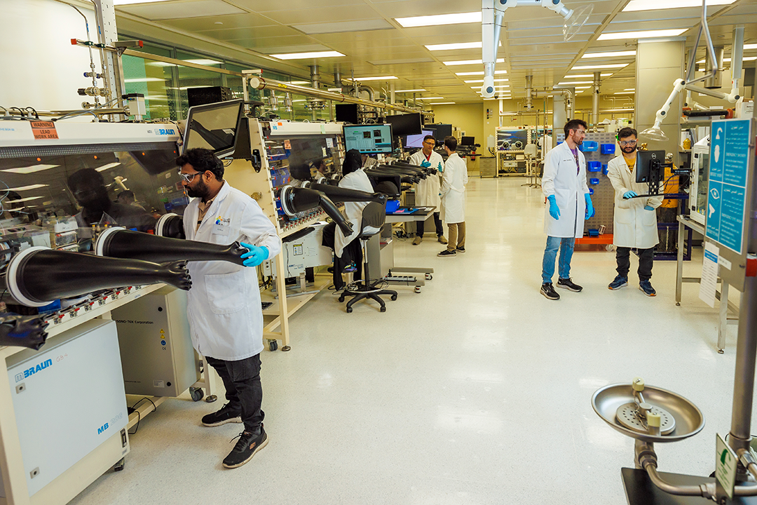
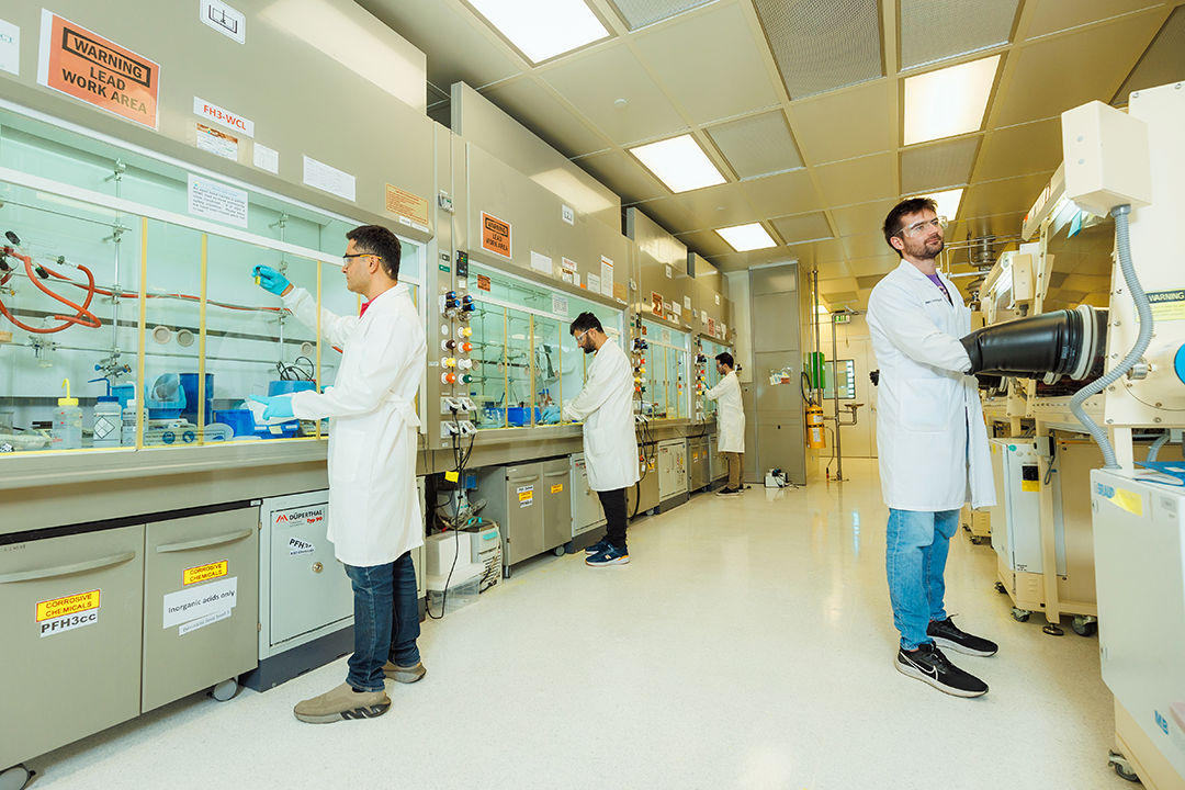
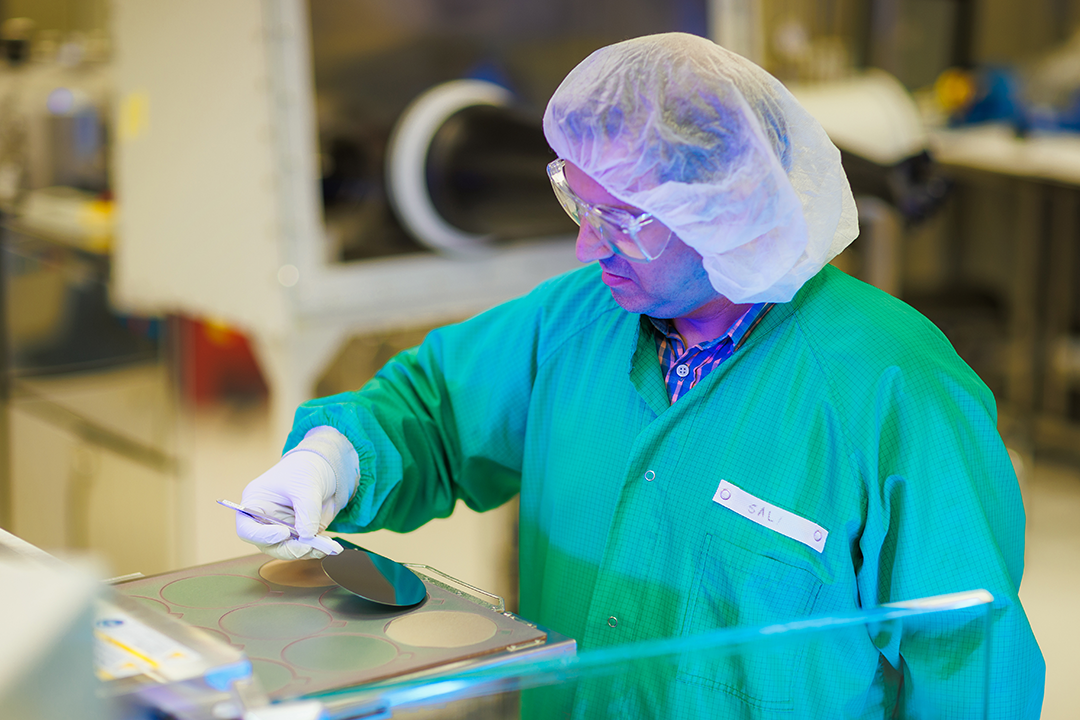
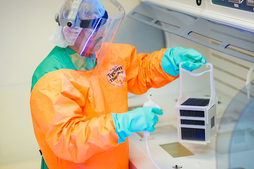
The Platform’s laboratories are a critical pillar of KAUST’s strategy and research capabilities. Its lab assets, together with KAUST's world-class Core Laboratories, empower faculty, researchers, postdocs, and students to push the boundaries in energy research and lay the foundation for future scientific discoveries. Specifically,the Platform’s state of the art laboratories, clean rooms and facilities that include physical and chemical vapor deposition systems and characterization facilities, ultrafast laser spectroscopy labs, device fabrication and characterization labs, and a wide variety of solution processing techniques.
KAUST Solar Platform
Plant Science Platform
KAUST Solar Platform
KAUST Solar Platform
KAUST Solar Platform
KAUST Solar Platform
Equipment
High-impact instruments supporting research
1. Thermal evaporators
Manufacturer: Angstrom Engineering
PVD chambers for depositing metals, metal oxides, organics, and perovskites
2. Sputter system
Manufacturer: Angstrom Engineering
PVD chambers for depositing metals and metal oxides
3. Plasma-enhanced chemical vapor deposition
Manufacturer: Indeotec
Deposition of thin-film semiconductors
4. Industrial module-scale solar simulator
Manufacturer: Eternal Sun B.V.
2300 × 1200 mm testing area; temperature range: 25 C to 90 C
5. Scanning electron microscope (SEM)
Manufacturer: Zeiss – Auriga
High-resolution SEM equipped with EDS
6. Atomic layer deposition
Manufacturer: Picosun
Highly controlled thin-film deposition method
7. Atomic force microscope (AFM)
Manufacturer: Bruker – Dimension Icon with Scan assist
Investigates film surfaces at nanometer-scale resolution
8. Hyperspectral luminescence imaging microscope
Manufacturer: Photon ETC - IMA VIS
Spectral range: 400–1000 nm; spectral resolution < 2.5 nm
9. Near-field spectroscopy system (nano-FTIR)
Manufacturer: nea spec - neaSNOM
Spectral range: 650–2200 cm⁻¹; up to 1 mW laser power
10. Photoemission spectroscopy in air
Manufacturer: Riken AC-2
Measures a material’s work function (3.40–6.20 eV)
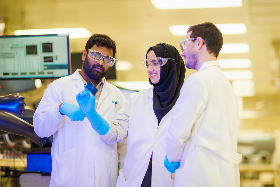
Team expertise
- Affiliated Faculty
- Platform Staff


Research expertise
Resilient Solution-Processed Photovoltaics:
Perovskite/Silicon Tandem Solar Cells:
Single and Multi-Junction Organic Solar Cells:
Platform Leadership Committee

CHAIR, PROFESSOR
STEFAAN DE WOLF
Material Science and Engineering

PROFESSOR
OSMAN BAKR
Material Science and Engineering

ASSOCIATE PROFESSOR
DERYA BARAN
Material Science and Engineering

ASSISTANT PROFESSOR
SHADI FATAYER
Applied Physics
PROFESSOR
QIAOQIANG GAN
Material Science and Engineering

PROFESSOR
MARTIN HEENEY
Chemical Science